DCM
Displacement Current Measurement (DCM)
1. Introduction
We, TOYO Corporation, have been engineering and marketing many test solutions to serve the liquid crystal display (LCD) industry for some time now [1]. We are also developing next-generation products by using displacement current measurement (DCM) technologies for evaluations of Organic Light Emitting Diodes ((OLEDs), Organic Photovoltaics (OPVs), and other materials with a TOYOTech LLC* member. On this page, we introduce the recent progress of DCM measurements.
2. About DCM measurement [2]
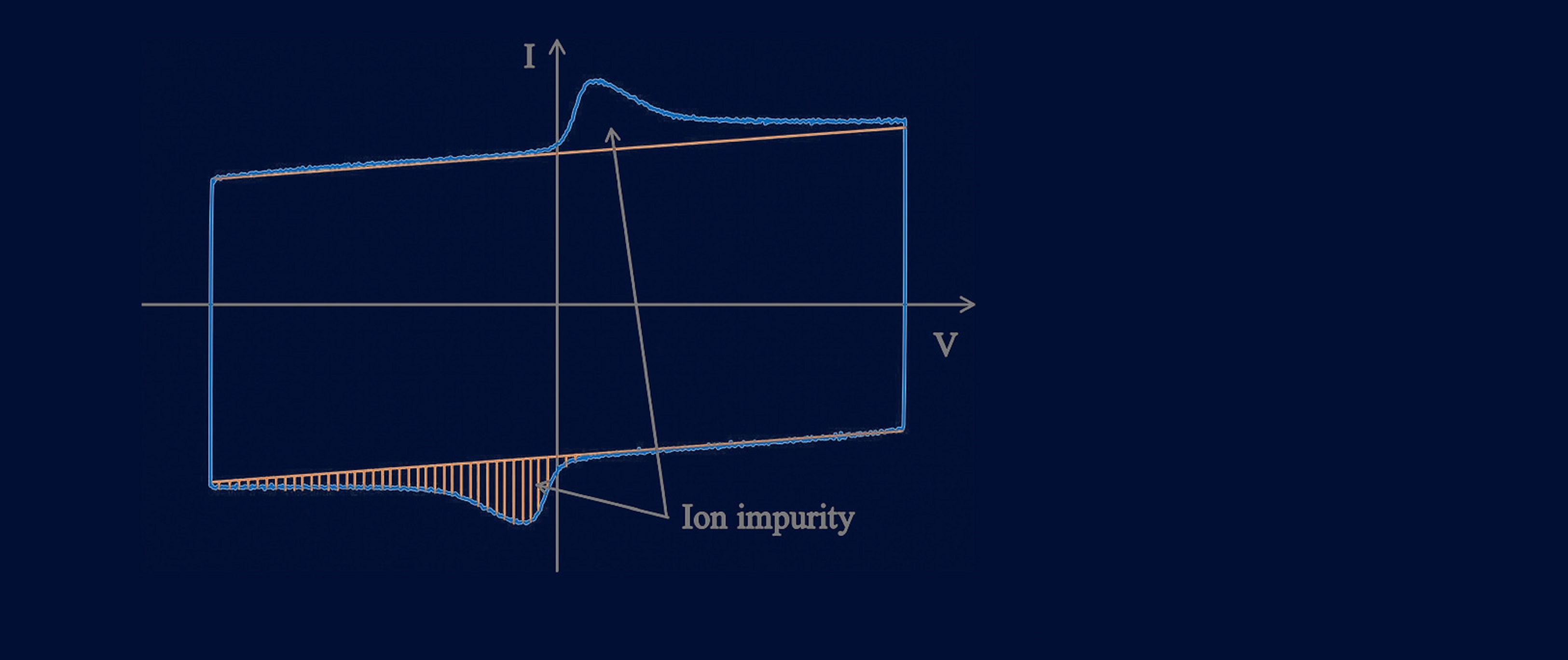
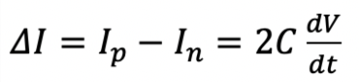
Figure 1(a) shows the equivalent circuit of a DCM for a CR sample having a parallel connection of resistance and capacitance. A triangle waveform voltage is applied to a CR sample, and voltage vs. current characteristics are obtained as shown in Figure 1(b). From the theoretical point of view, the total current (I) which flows through a capacitance (IC) and a resistance (IR) is defined by
 |
(1) |
In the case of dV/dt > 0 and dV/dt < 0, the currents of a positive slope (Ip) and a negative slope (In) become
 |
(2) |
 |
(3) |
Thus, the difference between Ip and In is proportional to the capacitance as shown in equation (4).
 |
(4) |
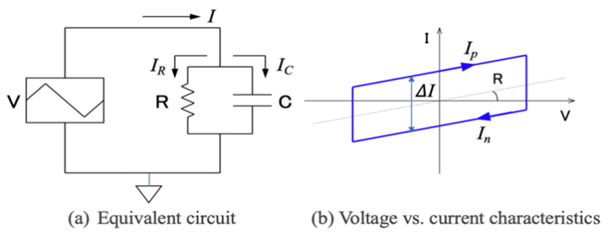
Figure 1 DCM: (a) Equivalent circuit of CR sample measurement by applying triangle waveform voltage and (b) typical voltage vs. current characteristics of CR sample.
3.Measurements
3-1. Organic Photovoltaics powders in a solvent [3]
This is joint research with Osaka Prefecture University. Figure 2 shows the equivalent measurement circuit of the ion impurity in a solvent. A triangular voltage waveform is applied to the test cell which is injected with a solvent with organic materials to be tested, and the displacement current is measured using a current to voltage amplifier and a voltmeter. Measurement data are plotted by voltage versus current characteristics as shown in Figure 3. If there is no ion in a solvent and organic material, two parallel lines are having a slope that corresponds to a dielectric constant and resistivity of a solvent and organic material. If there are ions in a solvent and organic material, these ion moves during voltage application and reach the surfaces in a test cell, and detect current peaks as charges, which corresponds to the amount of ion impurity. Normally, there are two current peaks with the same amount in positive and negative currents if a test cell has a symmetric structure.
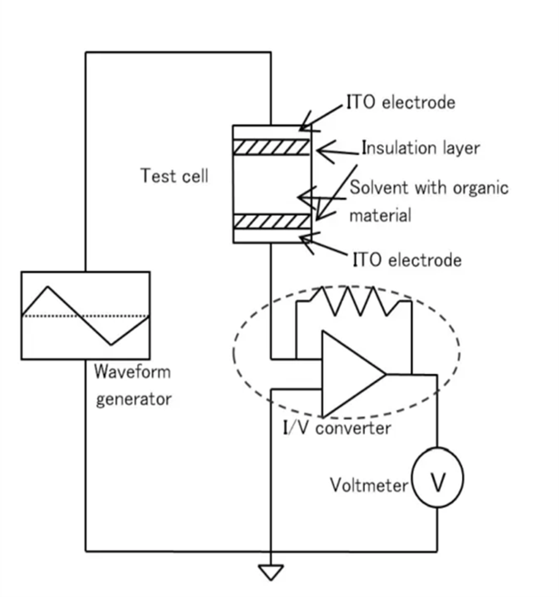
Figure 2 Equivalent circuit for ion impurity measurement of materials in a test cell
Figure 3 Schematic representation of triangle waveform voltage vs. current characteristics
Figure 4 shows the measurement results of different P3HTs in chlorobenzene solutions. We obtained the different amounts of ion peaks. Figure 5 shows the comparison between ion impurity amount and power conversion efficiencies which were obtained from OPV characteristics. We confirmed that the ion impurity amount in materials has a strong influence on OPV characteristics.
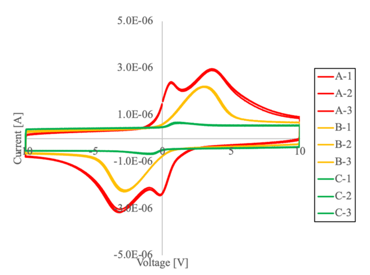
Figure 4 Ion impurity amount (peak area) comparison in P3HTs
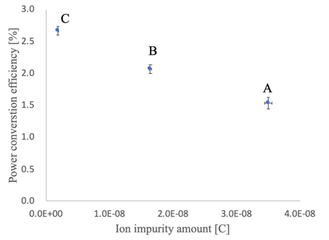
Figure 5 Correlation between ion impurity amount and power conversion efficiency
3-2. OLED powders in a solvent [4]
This is joint research with LG Display. We measured the ion impurities in TADF green powders in a Xylene solution and OLED device lifetime as shown in Figure 6. We found that there is a strong correlation between the ion impurities and the OLED device lifetime.
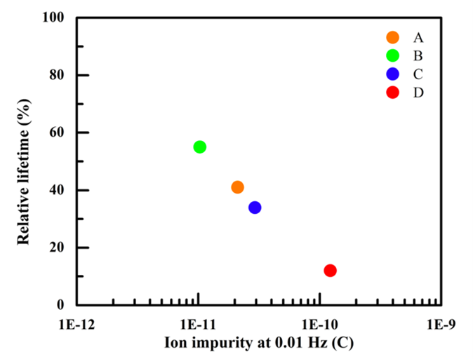
Figure 6 Correlation between the ion impurity in Xylene solution and the device lifetime
3-3. OLED devices [2]
This is joint research with Fukuoka i3-Center for Organic Photonics and Electronics Research (i3-opera). Figure 7 shows the equivalent circuit of DCM for OLEDs. The triangle waveform voltage is applied to an indium tin oxide (ITO) electrode on a glass substrate and measures a current from an aluminum (Al) electrode on organic material(s) with or without a LiF layer by using I/V converter. Figure 8 shows the measurement result of cyclic-DCM of OLEDs with and without a LiF layer. No significant difference of positive and negative currents between -5 V and -2 V for both OLEDs was observed, while both currents start to increase at -2.2 V and -1.8 V without and with a LiF layer, respectively. It suggests that the hole injection from an ITO layer to an α-NPD layer started around -2 V, and the LiF contributed to the reduction of the hole injection voltage by means of an increment of the injection barrier. Further, the current of OLED with a LiF layer drastically increased from +3 V, while the current of OLED without the LiF showed a bump between +2 V and +4.5 V, and increased at +5 V. It is obviously suggested that the LiF contributed to the reduction of the electron injection voltage from +5 V to +3 V, having efficient electron injection characteristics.
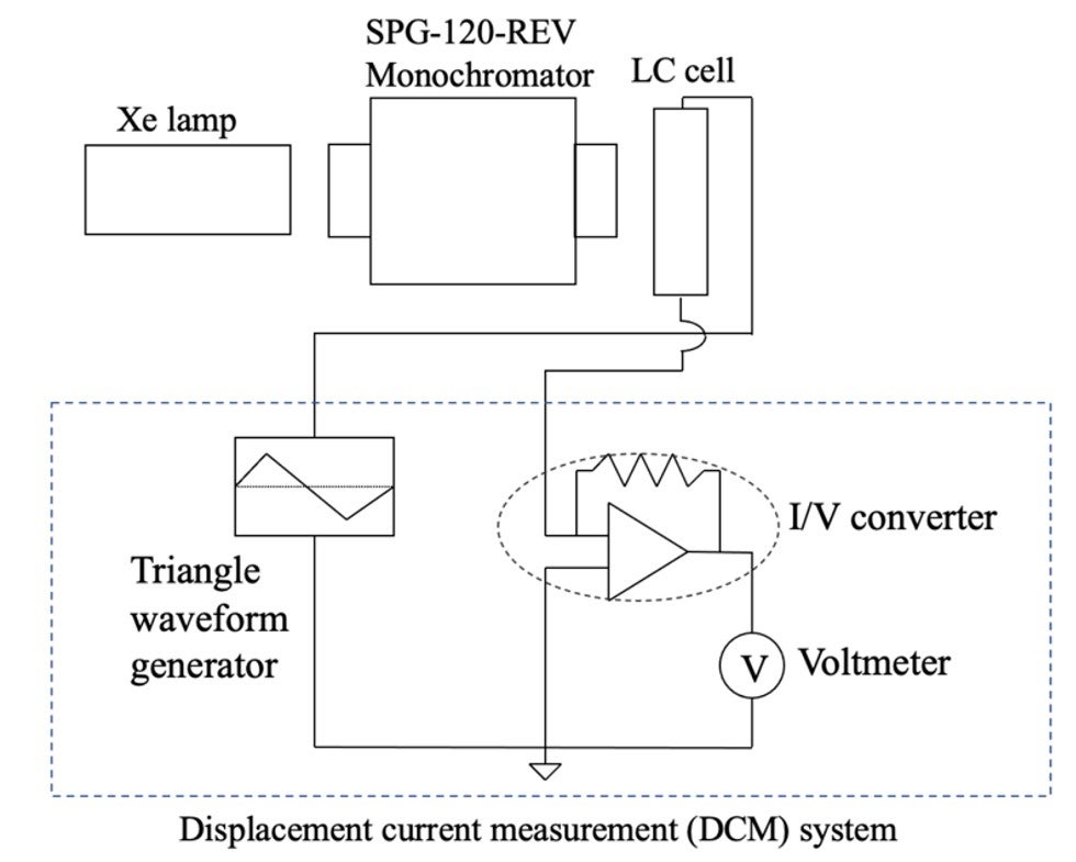
Figure 7 Equivalent circuit of DCM for OLEDs
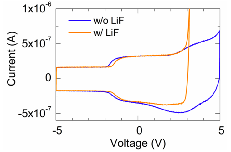
Figure 8 Comparison of DCM for OLEDs with and without a LiF layer on a TPBi layer
3-4. Thin films for OLED [5][6]
This is joint research with Japan Advanced Institute of Science and Technology (JAIST). Figure 9 shows the schematic representation of the sample used for DCM of thin films and the meanings of current peaks. The measurement conditions of DCM were set to 1 mHz of triangular wave voltage signal with ±15 V of applied voltage. The I-V characteristics were measured at temperatures of 25 and 80 °C. Figure 10 shows the I-V characteristics of the unpurified α-NPD and the sublimated α-NPD. In the I-V curve for the sample with sublimated α-NPD, no current peak caused by ions was observed. At voltages above ±10 V, the current gradually increased at 80 °C. This may be an indication of the initial stage of dielectric breakdown. On the other hand, the I-V curve of the sample with unpurified α- NPD shows a clear increase in the current at around -5V. Since no increase in current was observed at +5 V, the increase in current can be ascribed to the positive ions accumulating on the surface of the insulating layer.
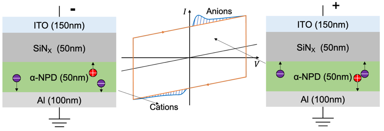
Figure 9 Sample structure to be measured and the meaning of current peaks
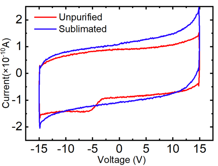
Figure 10 Voltage vs. current characteristics
3-5. Photoinduced charge in LCs [7]-[9]
This is joint research with Advanced Materials and Liquid Crystal Institute, Kent State University (KSU). We employed SPG-120-REV Motorized Compact Monochromator with Xe lamp (Shimadzu Corporation) and DCM measurement system for photoinduced charge measurement in LC cells. Figure 11 shows the block diagram of the measurement. We irradiated the light from Xe lamp to cells through the monochromator that can scan the wavelength from 280 nm to 780 nm by 10 nm step. We applied a triangular waveform voltage to LC cells and measured the displacement current to obtain the total charge which is calculated from the entire area of voltage versus current curve in LC cells on each wavelength. A photoinduced charge on each wavelength is calculated from the difference of total charge between with and without light exposure conditions. Figure 12 shows the wavelength dependency of photoinduced charge of LC mixtures from 280 nm to 780 nm by 10 nm step. We found that the photoinduced charges of each LC mixture started to increase at 700nm and drastically increased in the UV region. We also confirmed that the sudden increment wavelengths of photoinduced charge at the UV region of 5CB and MLC2132 were 330nm and 350nm, respectively. These results suggest that there is an inherent wavelength of the increment of photoinduced charge which is sensitive to the degradation of an LC mixture.
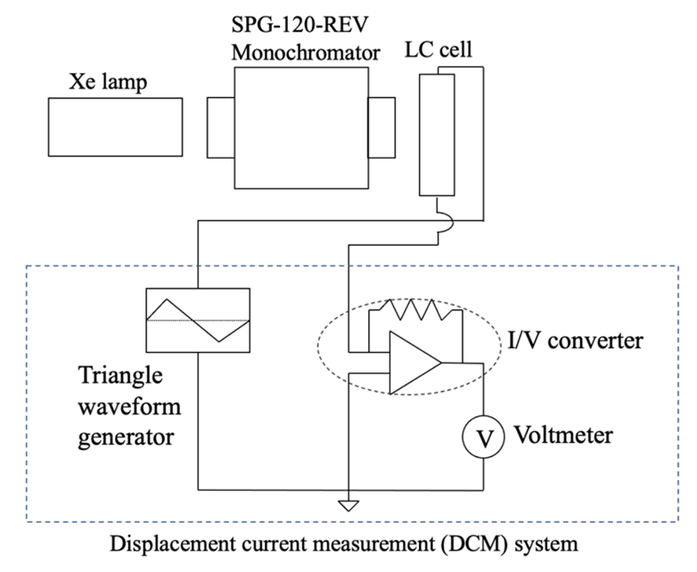
Figure 11 Block diagram of a photoinduced charge measurement
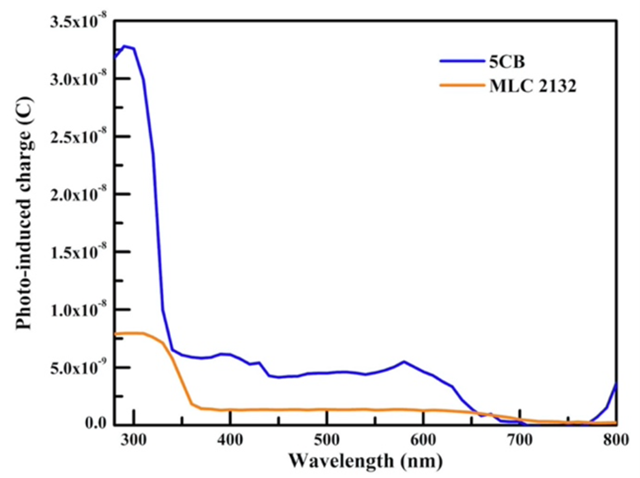
Figure 12 Wavelength dependency of photoinduced charge of LC mixtures
4.References
- [1] Inoue M. Review of various measurement methodologies of migration ion influence on LCD image quality and new measurement proposal beyond LCD materials, J Soc Inf Disp. 2020; 28(1): 92-110.
- [2] Inoue M, Kaneko Y, Fujimoto H, Miyazaki H, Adachi C. Evaluations of Lithium Fluoride Behavior in OLEDs by Means of Cyclic Displacement Current Measurement Method. SID Digest. 51(1), 2107-2110; 2020
- [3] Inoue M, Oyabu N, Kumoda Y, Suenaga Y, Ishii T, Naito H. Novel measurement method of ion impurity in OPV materials. Proc of AM-FPD’19, P-14; 2019.
- [4] Inoue M, Oyabu N, Kaneko Y, Kim J-Y, Yang J-H. Correlation between ion impurity in thermally activated delayed fluorescence organic light-emitting diode materials and device lifetime. DOI: 10.1002/jsid.922
- [5] Iwata T, Inoue M, Oyabu N, Ohdaira K, Murata H. Detection of Ion Impurities in Organic Thin Films by Displacement Current Measurement Method. SID Digest. 53(1), 1513-1516; 2022
- [6] Inoue M, Oyabu N, Iwata T, Ohdaira K, Murata H. Ion Impurity Measurements in Organic Thin Films on High Voltage Application. IMID2022 Digest, P2-165; 2022
- [7] Inoue M, Kundu S, Yokoyama H. Photoinduced Charge Behaviors in Liquid Crystal Mixtures. Proc of IDW’20, 129-130; 2020
- [8] Inoue M, Kundu S, Yokoyama H. Photoinduced Charge Behaviors in Liquid Crystal Mixture on Different Measurement Frequencies. Proc of OLC’21, P29; 2021
- [9] Inoue M, Oyabu N, Kundu S, Yokoyama H. Correlation between Photoinduced Charge and Cell Resistance in the LC cell. Proc of ILCC2022, PF.301; 2022